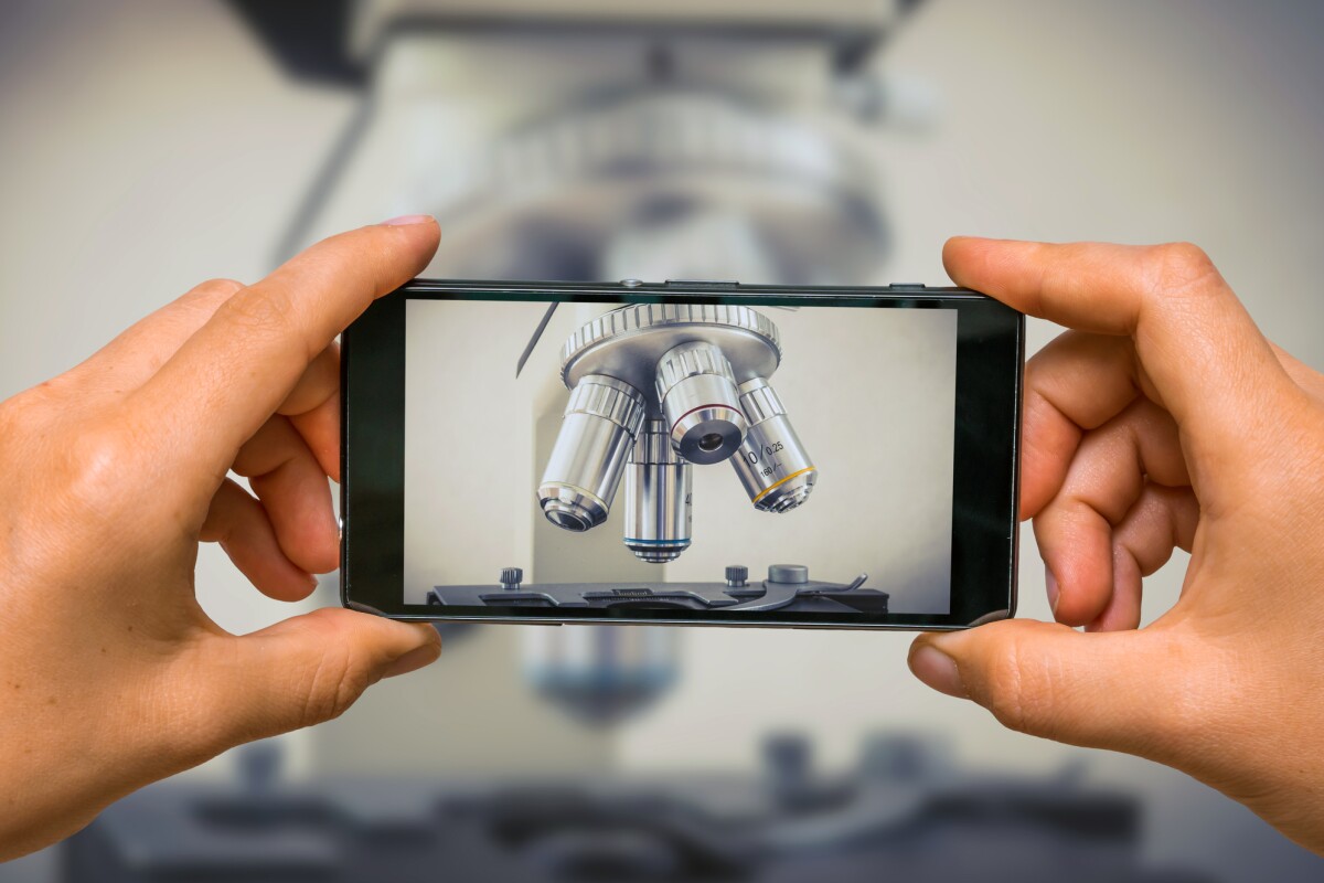
Researchers have created the world’s smallest silicon LED and holographic microscope that opens up a wide range of potential applications, including turning your smartphone camera into a portable, high-resolution microscope.
Photonics is the area of technology concerned with the transmission and properties of photons. Developments in photonics have led to innovations across a wide range of fields including optical data communications, imaging, life sciences and healthcare, and lighting and displays.
But off-chip emitters may be a thing of the past, thanks to researchers from the Singapore-MIT Alliance for Research and Technology (SMART) who’ve developed the world’s smallest silicon light-emitting diode (LED) – at less than a micrometer wide – with an intensity comparable to much larger silicon LEDs.
Previous on-chip emitters have been difficult to integrate into standard complementary metal-oxide-semiconductor (CMOS) platforms. CMOS is an integrated circuit built on a printed circuit board, the semiconductor technology used in most of today’s chips. In mobile phones, CMOS is used as the ‘eye’ of the camera.
Here, the researchers placed their tiny silicon LED in a 55 nm CMOS node alongside the other photonic and electronic components – all on one chip.
To test how their LED might be used in a real-world situation, they placed it into a lensless holographic microscope. Lensless microscopes are smaller than regular microscopes and less expensive because they don’t require complex, precise lens systems. They use a light source to illuminate a sample; the light is then scattered onto a CMOS digital image sensor, creating a digital hologram that a computer processes to produce an image.
There can be difficulties with lensless holographic microscopy in reconstructing an image. Usually, an accurate reconstruction requires detailed knowledge of the aperture and wavelength of the source light, and sample-to-sensor distance. To counter this difficulty, the researchers used a neural networking algorithm to reconstruct objects viewed by the holographic microscope. Neural networks are computer systems that mimic the networks of the human brain, relying on training data to learn and improve their accuracy over time.
The researchers found that their holographic lens provided more accurate high-resolution images than a regular optical microscope. They calculated that its resolution was approximately 20 micrometers (microns). For context, a human skin cell is 20 to 40 microns across; a white blood cell is about 30 microns.
The researchers see many applications for their next-gen CMOS-integrated micro-LED and neural network, including reconstructing microscopic objects such as human tissue samples and plant seeds. And the researchers say it can be used in existing smartphone cameras simply by modifying the phone’s silicone chip and software, converting the phone into a high-resolution microscope.
“On top of its immense potential in lensless holography, our new LED has a wide range of other possible applications,” said Rajeev Ram, corresponding author of the study. “Because its wavelength is within the minimum absorption window of biological tissues, together with its high intensity and nanoscale emission area, our LED could be ideal for bio-imaging and bio-sensing applications, including near-field microscopy and implantable CMOS devices.”

